Mid-Power HF Amplifiers
When out on mobile radio trips I dream about a big signal to shout back at the DX I can hear (SSB). My Elecraft KXPA100 is wasteful, like all class-AB designs. It also needs a healthy 13V+ supply to get a full 100W output, whereas a good car battery drops to <12.5V off charge. Some amateur class-AB amplifiers are still in the 1980s with obsolete IRF510 or Motorola RF parts!This page looks at two designs of HF amplifier for mobile/portable operation.
100W Class-AB for IC-705/KX3/FT-818 (2020-)
I’m designing with a 36V battery as an accessory for the IC-705 radio. It will also work with the Yaesu FT-817/818 or KX3 with a suitable cable for the PTT signal. The feature set:
- Field replaceable power-tool lithium-ion battery packs
- Higher efficiency power stage with fewer parts
- Auxiliary 13.6V, 2.0A output for IC-705/FT-818/KX3
- Improved mechanical assembly and heatsinking
- Open source hardware designed with KiCAD
- Correction of previous circuit and PCB issues
- Updated microcontroller for more accurate current & voltage measurement
- Added input power and efficiency display
- Revised input circuit for full 100W from 1.0W drive
THIS PROJECT IS NOT FINISHED. Selling ham radio kits is a money-loser and very time consuming, time which is better spent on designing future projects. There are various companies that will produce PCBs and populate with SMD parts, like this and this. Then the rest of assembly is to wind the magnetics and fit them, plus half-a-dozen other through hole parts.
The hardware design is open source in KiCAD8 format. I no longer provide Gerber/Excellon files, as KiCAD is free to download and works on Mac OS/Windows/Linux. The following file is dated April 2024 to include all improvements:
KiCAD hardware file, includes PDF circuit
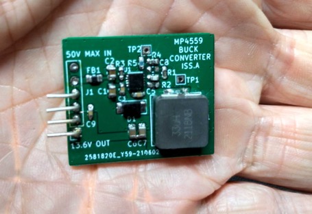
The proximity of the buck converter near the MRF101 FET always caused concern because of heat from the output stage. The buck power module was moved to a separate PCB and changed to an LMR38020 chip which is easier to handle than the MP4559. These 2 chips both perform OK, the LMR38020 slightly cheaper as it lays out onto 2-layers.
The MP4559 PCB performs well - 13.6V output at 1.5A, good regulation and ripple, 700uA quiescent current. The PCB design pack and photo follows:
KiCAD hardware file for buck converter
Construction and firmware work on Issue F PCBs is continuing as shown here:
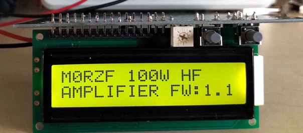
Issue F PCB changes include: removal of the rotary encoder in favour of cheaper more easily available switches; Facility to reset the LCD display; Buck power module moved to external PCB; Update to KiCAD8 format; Correction of several silkscreen issues.
The circuit needs 36V power, from either a 36V pack (typically made by Bosch) or two 18V packs in series. The 18V packs are more common. It can also use a 36V scooter battery. Depending on the battery capacity, transmit time on 25% duty SSB will be over an hour, perhaps 2 hours. On receive current drain drops to a few mA.
A stack of 10 18650 batteries give 36-42V. 2Ah capacity is conservative, but the cells need high drain capacity. The latest cell from a reputable manufacturer (not Chinese) is e.g. the Murata VT5D with 2.8mAh capacity. Constructing interchangeable packs and chargers for stacks of cells is extra work, and I decided to use the replaceable packs instead.
Battery adaptors are available for DeWalt/Makita/Bosch packs and two fit perfectly under the 160mm long case of the amplifier. Making the whole 100W amplifier a tidy and robust package. Here’s a photo of the general construction:
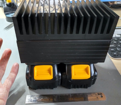
At 160 x 160 x 100mm it looks big with two DeWalt packs underneath. But these are 5Ah batteries that give operating time over 2 hours (depending on Tx duty) and also keep the auxiliary radio battery charged. The 2.0Ah batteries are slimmer and easily support 1 hour SOTA activation.
Technical Description
The concept is to provide advanced features and remove expensive parts. The encoder of prototypes was removed in favour on push buttons which are cheaper and better. The MSP430 capture unit is a frequency counter for band selection, avoiding band selection switches on the front panel. Automatic bias adjustment avoids manual potentiometers.
A 16x2 (1602A) LCD is the cheapest way to display the information. These modules are made in China at low cost and high volume. The display enables the secondary feature of copy protection too. The trimpot for contrast adjustment is more expensive than a DAC for contrast adjustment, perhaps in future I should do it that way. The LCD is used in 4-wire mode to save pins. These LCDs need an ICL7660 charge pump inverter fitted for their LCD bias
The MSP430 does all monitoring and control, like Rx/Tx sequencing and fault protection. The main defence against faults is simply switching back to receive. The main risk with that is welding the output relay if it switches at a peak of power. So the MSP430 does a sequence of reducing gate bias to zero and cuts off the boost power module, then waits 4ms before switching the Rx/Tx relays.
The MSP430 capture unit is a frequency counter for automatic band selection. If operation on a different band is detected while the amplifier is in transmit, it returns to receive mode to protect the band switching relays. Changing bands while transmitting is locked out on most radios anyway. The MSP430 has a maximum logic speed of 16MHz, so a divide-by-2 gate is used to bring down the possible 29.7MHz input to below 15MHz where the capture/compare is happy with it. The limiter circuit supports 0.5W-10W input power. The input power is also monitored.
The software reads the supply current, forward/reverse power, input signal magnitude, supply voltage, and temperature sequentially every 1ms. It also sends characters to the LCD at that rate and checks for button presses. Fault conditions have to be seen on 2 adjacent cycles to register as a fault. Every 50ms the auto band selection frequency and temperature are checked. Until the band selection count has been registered twice, band switch is not made. The MSP430 runs at 8MHz but enters sleep mode once its processing cycle is complete. During sleep the ADC unit is reading the ADC channels.
Current monitor of the power stage is through an INA290 and 20m-ohm resistor. The INA290 produces an analog output within the range of the micro's ADC circuit. Large reservoir capacitors 1000uF x2 are provided to handle the highest current peaks.
Input signal magnitude is measured to avoid overdriving the input. LDMOS FETs are sensitive to being overdriven. If input power is excessive the unit does a return to receive mode sequence. The magnitude is carefully split from the drive to the frequency counter.
Temperature Monitor
An TC35A5 temperature sensor is fitted close to the power FETs. The temperature is read via I2C bus, and displayed on the LCD. The MSP430 uses the temperature reading to reduce bias when the FETs are hot. It also returns the amplifier to receive if the reading is above 90C.
Lowpass Filters
A 6 section switched low pass filter covering 160m to 10m is onboard. The bands are selected directly by micro logic outs. The filters are uprated versions of designs used on previous amplifier projects.
SWR Bridge
A “tandem-match” SWR bridge. It needs 15 turns to present enough impedance on 160m. The bridge produces >3.3V, so a resistive divider follows to reduce voltage within the range of the microcontroller.
Software Operation
The issue B and C/D boards differ in the microcontroller changed from an MSP430G2453 to an MSP430FR2155. The software is written in Code Composer Studio (CCS) using the ‘C’ language. The code is in .txt format and can be programmed in with any MSP430 programmer supporting Spy-BiWire 2 pin programming, like MSP-FET
Once programmed and run the software shows two 4-digit numbers. The buttons move the cursor and increment/decrement the values. The process to unlock the software follows:
- Email me the 4-digit code on the top line
- I send an unlock code back
The software is not open source, and once the project is completed I will be charging to unlock the unit.
The LCD top line shows the amplifier status: TRANSMIT/RECEIVE/BYPASS
TRANSMIT (transmit mode with no faults)
RECEIVE (receive mode or return from Tx to Rx due to: hi-SWR, hi-curr, ovr-temp, ovr-volt, hi-input)
BYPASS (the PTT line is disabled and transmit power is passed straight through)
Pressing up/down buttons scrolls the bottom line through these pairs of values:
PEP SWR (peak power output and SWR, zero on receive)
VLT CUR (supply voltage and PA current)
BND TMP (auto-band selection and temperature)
PIN EFF (power in and efficiency)
Pressing the buttons or going into transmit makes the LCD backlight come on for 30s. This is done to save 40mA of backlight and relay current in long receive standby periods. Current with backlight off is <2mA. A fault condition latches in for 20 seconds and switches to receive. Keying to transmit is not possible during this timeout.
A footnote on alphanumeric LCDs: The present ‘1602A’ LCD sold in volume from China is slightly smaller than the 1602 LCD that was prevalent 10 years ago. As often happens with far eastern electronics, someone designed a PCB (with some jarring fonts!) then everyone else copied it. A quirk with these boards (not documented elsewhere) is that they don’t like to be initialised twice. When using a debugger, initialisation code is run every restart, resulting in garbage shown on the display. I had to add a power control circuit to give complete reset and ensure the display comes up properly.
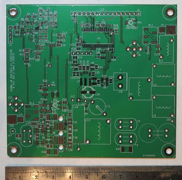
Issue B PCB Design (2019)
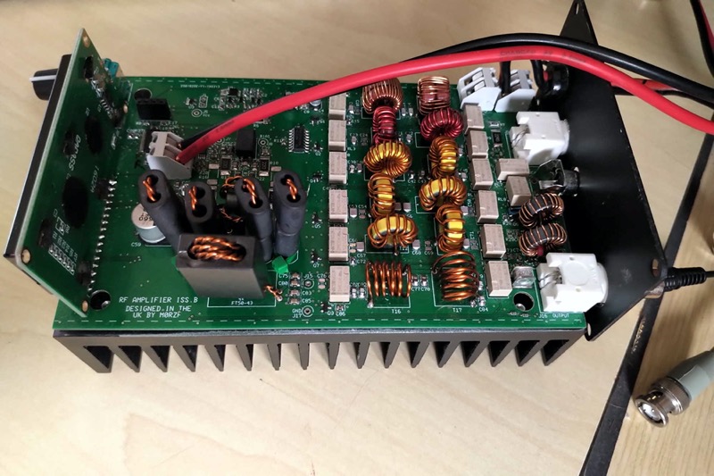
Ground-work was done for auto-band switching; SWR protection and monitoring; boost power supply; Low pass filters; output transformers. The amplifier was a minimal parts count 100W (PEP) amplifier with similar functionality to the Elecraft KXPA-100 but with far fewer parts. Prototype hardware photo:
Hardware Description
Connections are:
DC Input power, 20A maximum, 15A average
RF in BNC, 1.5W maximum
RF to antenna BNC, SWR 2.5:1 maximum
PTT phono socket, short to ground on transmit (provided on many radios)
The amplifier needs a 30V power supply, which can be made by “600W” boost modules available on eBay or Amazon. I found these modules to be very noisy and based on older technology (TL494), resulting in poor efficiency. They have no current limit or over temperature protection.
Besides the awkward boost converter from 13-30V, many other problems with this design resulted in these updates:
* Obsolete MSP430G micro replaced with MSP430FR family
* Removal of lossy resistive input matching to allow lower consumption drive from transceiver
* Replacement of IN4007 with S1D SMD diode
* Replacement of INA138 current monitor with INA290 for better range and accuracy
* Replacement of NXP temperature sensor with TC35, cheaper and I2C performance more stable
* More pins on new micro allow removal of &4HC238 decoder and drive LPF selection directly
* Re-layout of tandem-match SWR bridge with smaller toroids
* Improved frequency counting and 3.3V stability with revised limiter circuit
* Use NCP718x regulators for improved input range and lower supply noise
Power Stage
Here are some secrets of HF PA design not often written in textbooks. The power stage is based on NXP MRF101A/B LDMOS transistors. A mirrored pair is used to improve the PCB layout, as the gates and drains are adjacent. The FETs are placed to be thermally attached to a large heatsink. Balanced layout is essential with this type of design, it spreads the power dissipation across 2 semiconductors, balances out 2nd harmonic, at the expense of a small increase in complexity.
The supply voltage sets the matching impedance. With a 1:4 transformer and 110W out at 28V supply, the impedance is about 12.5Ω assuming saturation voltage of 0.5V. That ratio enables a 1:4 transmission line transformer, far lower loss and lower cost than the dreadful tube-in-bead design. Alternatively a 1:1 transmission line (RF choke balun) can be used with a 36V supply and a low-pass filter with 25Ω to 50Ω impedance match. 36V is an odd voltage available from power tool batteries, Bosch/Makita/Dewalt. The 2nd of these choices removes a transformer, and is an ideal concept for a battery-portable amplifier.
At the input there is a min-loss-pad of 2dB which reduces the input impedance to 25Ω. That reduces the chance of overload at the input and ensures a reasonable match to the driver transmitter. 25Ω also helps broadband matching of the capacitive FET input. A balancing choke T3 ensures the 2 FETs are driven 180 degrees out of phase. The transformer is a ready wound part to cut costs. The input bias to the FETs comes from an MCP47FEB 10-bit DAC. The DAC is controlled by the MSP430 to give correct bias without manual adjustment. The bias is dropped down slightly at high temperatures.
The FETs drains are fed by a balancing choke which has 2 purposes. It ensures that the dc and ac supplied to the FETs is equal and opposite - i.e. balanced. A small amount of negative feedback is tapped off by a single turn thru T8 and connected to the FET gates. The feedback reduces distortion and gain. Gain is plenty high enough so a few dB reduction helps.
Input switching is with S1D diode, actually a rectifier but works fine as a switch. Output of the power stage is switched with an Axicom IMC06 SPDT relay, which has highest current handling in a small package.
Zero-Z (zero output impedance) HF Amplifier (2020-)
The high efficiency HF amplifier is now called Zero-Z: snappy and describes what it does.
HF amplifiers are designed around 50Ω impedance with linearly operated semiconductors. That gives them a maximum efficiency of 50% with a 50Ω antenna. Clearly it’s not good to transmit 100W and waste 100W, and at lower output they are worse!
SSB transmission is far from ideal for a switching type amplifier, as phase and amplitude parameters must be maintained.
So far, I did some practical tests but a lot more simulation. Here’s a FFT spectrum in LTSPICE with 3kHz AM modulation. Peak power 130W from an 18V power supply at 94% efficiency. This design gives incredible efficiency from the semiconductors, 1W dissipation for 130W output. Made reality this allows a 100W+ amplifier with a small heatsink.
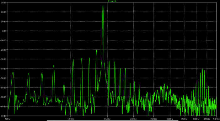
Though the result looks spiky, the spurious is <50dBc which is the required limit for ham radio equipment. This is only an AM modulated test, the next plot shows a 2-tone test (SSB) signal simulated in LTSPICE. The frequency is 14.2MHz.
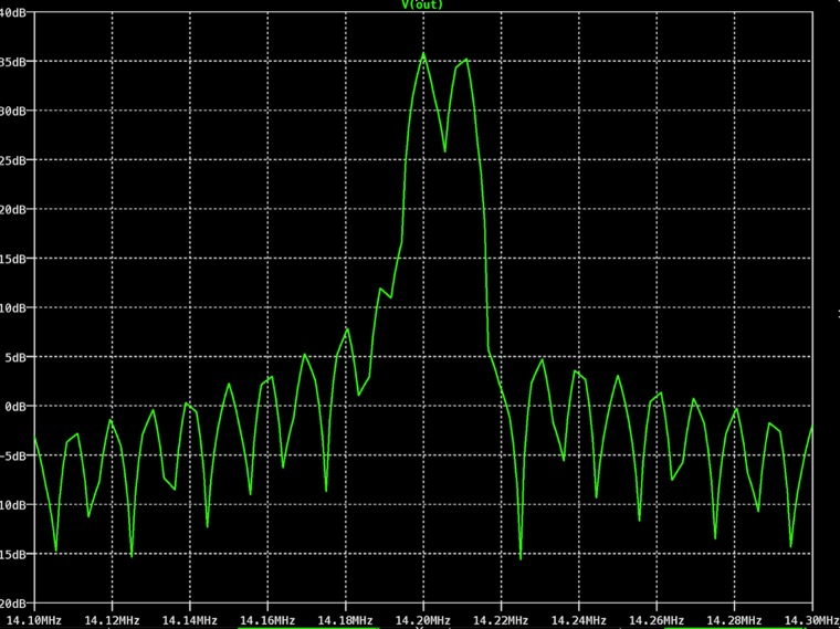
The FFT resolution of this 2-tone test is a coarse 4kHz on 10kHz spacing, and took a lot of processing to simulate, but shows the IMD at -30dBc. Another sim with an audio tone spacing of 2kHz showed it about -40dBc. The 2-tone waveforms in the time domain also show close reproduction between input and output. In other words no worse than a commercial class-AB transmitter.
Another issues with Class-E is maintaining the correct drain waveform over a wide range of load conditions (SWR). From simulation this means the optimum power output cannot be achieved. To cope with 2:1 SWR the drain waveforms must be run with negative excursions. GaN FETs do no have a body diode, so one must be added.
This is the first test PCB, which didn’t work well but was a major learning exercise.
Initial tests confirm high efficiency from the power stage, with 65W produced from 13.8V, 5.3A = 93%. Modulating this raw power yet keeping safety margins on the FETs is the challenge.
Much of the technology is new or not given in books anywhere. I found approaches to circuit design that overcome failures of previous experimenters with envelope restoration. An SSB amplifier can be made without generating the transmit signal as the Polar Explorer does, saving hugely on complexity. Simulations of these circuits look excellent, with 130W produced from an 18V pack. If simulations can be made into reality, a 130W HF SSB amplifier without a large heatsink and a lightweight battery for several hours operation is possible.
A high efficiency amplifier across the whole 160-10m frequency range becomes very complex, and may not be possible. So covering 2 bands at once is the best approach. Going above 20m with the topology looked at may not be possible. If anyone would like to collaborate on this project I can share more information privately than given here. Eventually I hope to release the hardware as open source, but the software will be closed/licensed as with the class-AB projects.
Realisable Efficiency
A practical amplifier needs a drive source, transformers, filters, ancillary circuits. Looking at power loss in a typical class-AB amplifier in terms of dB and percentage:
- 0.5dB = 12.5% loss in output transformer
- 0.5dB = 12.5% loss in output filters
- 0.4dB = 10% loss in switching and connectors/cables/PCB tracks
- The drain efficiency will be 60% at best, 40% lost
So for 100W, dc input power will be >160W and a 13V amplifier takes >12A current. For lower power output in class-AB efficiency drops substantially, down to perhaps 30%. SSB duty cycle is generally only 25%, so amplifier efficiency will be way below 50%.
Class-E and similar switching amplifiers are listed in books as >90% efficiency. There are extra losses in a practical system from the rest of the circuit. Getting overall efficiency above 80% maybe impossible given the constraints of all the passive circuit elements.
For the example of a 100W amplifier, it will pull 125W, or 7A from an 18V power supply. Better than class-AB, but there will always be some waste. Wastage is dependant on the power loss of every power handling component in the system. A zero-impedance transmitter stage is not realisable, but something close is.