Updated 20180823
A previous project was with low-cost (<£1) switching FETs to advance the art beyond the very cheap, barely functional Chinese products on the market. They promise 100W for low cost but cannot deliver half that, and are very crude, not even providing an Rx/Tx relay - buyer beware!
There's no major advance to be made in class AB amplifier design, but improvements in economy are possible. Problems with designing for the HF frequency range are:
- The industry is producing transistors for VHF and above…
- Which means those for lower frequencies are expensive
- Switching FETs are cheap but have many shortcomings
- Linearity issues
- Efficiency issues
The most common modern device for HF amplifiers of about 50W is the Mitsubishi RD70HHF1. They have some disadvantages:
- High cost >£30 each in small quantities
- Output impedance is low, forcing an inefficient 1:16 output transformer
- Doubtful linearity with 12V supply, see many rig reviews in magazines!
- Becoming obsolete
I looked through the enormous range of switching FETs available. These are the challenges of designing with them:
- High gate capacitance (except early generation e.g. IRF510), makes a flat 1-30MHz response difficult
- TO-220 packages with inductive wire bonds
- Switching FETs hotspot badly and the bias point is unstable… OnSemi, Infineon, Microsemi agree…
- Temperature compensation and other measures are essential
- The drain or tab is hot to voltage and RF
Many were investigated but these TO-220 packaged FETs are best suited - FQP13N10, IXTP2R4N50P. The Fairchild has a track record in citizen band radio output stages. The IXYS FET is obsolete, as Littelfuse acquired and closed the former IXYS semiconductor company.
DMOS power FETs can hotspot and burnout under continuous high current. So any amplifier like this must be rated in SSB for higher power than in CW modes like PSK31. Having neutralisation (feedback) from drain to gate is actually a form of bias. Having this allows the no-signal bias to be lower, giving the FETs a chance to drop well inside their forward bias safe operating area during speech pauses. I found the FQP13N10 stable with a heatsink of 1C/W, and bias of 250mA per device.
I looked at designing a boost power supply in TI WebBench. The cost of a 30V, 5A boost converter makes up half the price difference to using RD70HHF1 FETs in the first place. A solution was found in “600W" boost power supplies from China/eBay. These can give 150W if heat-sinked, and are voltage adjustable, with current limit for £6! With such a cheap way to get 30V @4A, plans for integrating a boost power supply were dropped. Having a boost module has several advantages -
- Operate at the same output power with 10-20V input voltage
- Improved efficiency output transformer
- Improved linearity at higher supply voltage
The boost modules use the old TL494 chip from TI. Its dead-time control provides shutdown during receive.
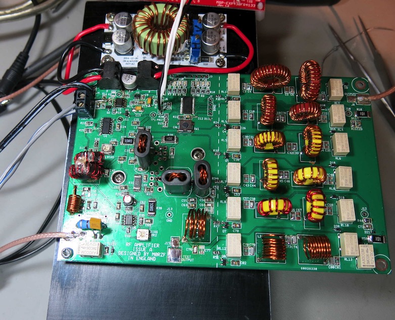
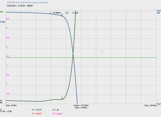
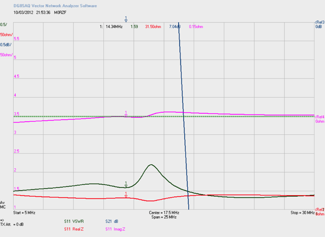
The amplifier diagram is here and here. I found IXTP2R4N50P FETs the best overall performers. FETs from St Micro and Infineon were also tested, but the Infineon (IRF520) part gave low gain. The ST part had a serious hot spotting and burnout issue. Here is the amplifier under test, with the Chinese boost module mounted next to the main board.
This project is now finished and a mini-movie is on Youtube. The play-safe RD16HHF1 version BOM is here.
Software - as mentioned on the video above, the software requires keying to transmit when first powered up. This measures the temperature compensation diodes and calculates the bias offset. Pressing the CAL button during transmit calibrates to the peak transmit power. Fitting a zero-ohm link across R22 forces the board to use a binary code on the BAND connection, instead of automatic band switching.
Due to Chinese rip-offs of ham radio projects, the software is closed source.
FQP13N10 Version
The RD16HHF1 FETs can only produce 20W, and that's with a healthy power supply of 14V. With the FQP13N10s and the voltage boost module, these results were measured:
80m, 6.2A, 35W
40m, 7.8A, 38W
20m, 9.0A, 40W
15m, 8.0A, 30W
10m, 6.0A, 25W
The centre column being total input current. The output will go higher, but it's not a good idea to push our luck with these cheap FETs. At 80p each, they are about 1/4 the price of the RD16HHF1's. FQP13N10 BOM HERE and circuit PAGE1, PAGE2
The FQP13N10 works up to 30MHz with 2-3dB less gain than at 3MHz. This is done with negative feedback to swamp Miller capacitance, and careful matching at the input. FQP13N10 gives 20dB+ gain at lower frequencies without compensation. With compensation, 13dB gain at 3MHz and 11dB at 30MHz was measured on prototypes.
It's important to consider the tradeoff of drain voltage headroom vs. drain-source capacitance. Increasing supply voltage pushes up the impedance and allows optimum choice of output transformer. Using a 1:1 output transformer pushes up peak drain voltage. At 40W into 50Ω, the drain voltage peaks at 64V (assuming zero saturation voltage). Any SWR above 2:1, especially inductive loads, will easily push the crest voltage >100V and blow a 100V FET instantly. This is why FET amplifiers can be sensitive to high SWR.
So why not just use a (12V) low voltage supply? The answer is found in this graph.
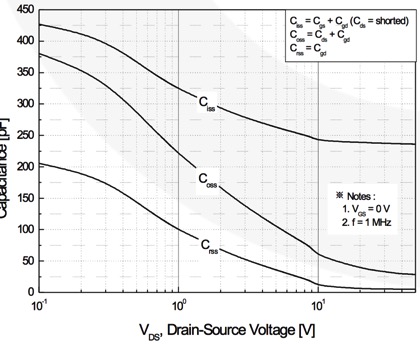
The horrible change of capacitance (Coss) of a FET causes non-linearity. Higher voltage FETs shift the above graph to some extent, so using a higher voltage FET to reduce intermodulation distortion is a trade-off of SWR tolerance against the non-linearity.
IXTP2R4N50P Version
The IXYS FETs are lower capacitance devices, and work really well up to 30MHz. Unfortunately they are now obsolete.
AFTER EXTENSIVE WORK WITH DMOS SWITCHING FETS AT HF, I CONCLUDE THEY HAVE MAJOR DISADVANTAGES!
Older Power Amplifier Designs (Deprecated)
Previously I designed amplifiers to produce 15-20W of RF power from less than 0.5W of drive. Targeted at Soft-rock project builders, though adaptable to boost other QRP or home-brew rigs to the 15-20W level. I added several unique options. All details are in the public domain. Anyone that wishes to build this design, get commercial standard PCBs made, or sell kits, is welcome to do so.
The final batch of PCBs for these boards is now sold out. This is the prototype undergoing tests:
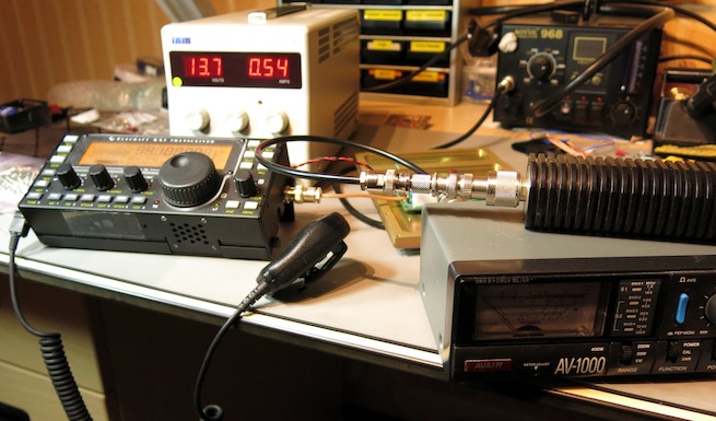
There is also a mini-movie here. It is being driven by an Elecraft KX3, set to 0.3W output. Voltage supply and quiescent current are seen on the power supply. In the foreground is an SWR/Power meter with a dummy load sat on top. The power meter indicates 15W output from a “whistle test”. The next photo shows the completed board mounted on a heat-sink plate:
It captures several years of design thinking, and has features not found on other similar amplifiers:
- The power MOSFETs have dual footprint, for Mitsubishi RD16HHF1 or power supply FETs
- Input PI network for matching circuit or attenuator
- Temperature compensation of bias to help stability
- Facility for single or multi-band filter
- Integrated RxTx relay with pull-low or pull-high switching voltage
- Options for external filter banks
Datasheet parameters to look for in switching FETs are low input capacitance (<350pF), Vds max >40V. Package TO-220 or TO-247. Most MOSFETs optimise RDSon and have high input capacitance. Check websites of ST, Fairchild, NXP, Texas Instruments, On Semiconductor, International Rectifier, Vishay, and others. New types of MOSFETs often come onto the market.
The Kits & Parts single band filter is no longer available. I have some replacements.
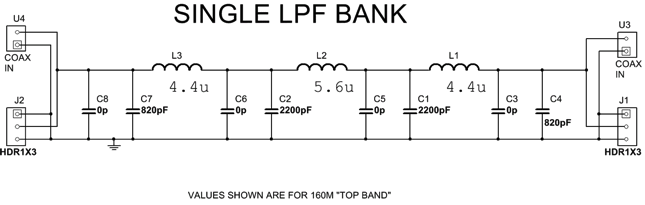
The bare PCB:
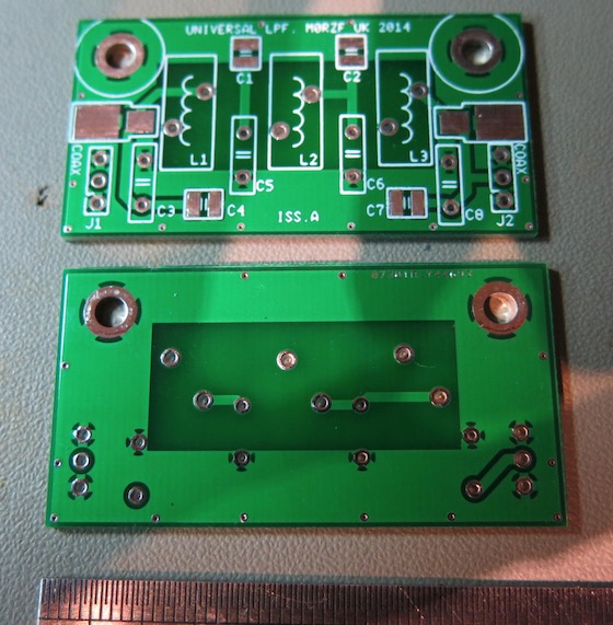
There are several options for external filter banks on the amplifier PCB. An external higher power amplifier can also be used. Look at the circuit diagram and see what is possible. That’s why there are several coaxial termination pads on the board. Anyone that builds this amplifier, then wants to cover more bands with automatic switching, can add an external board. If there is demand I can design a suitable filter bank. My previous design had 4 filter banks, and worked fine from 80m-15m.
If you want better efficiency on the bands <10MHz it is possible to use a BN43-202 twin hole ferrite rather than the type 61 ferrite.
Also there’s an option for a TMP100 temperature sensor, controlled by I2C. MoBo V4.3 users may find it useful to read the output PA temperature instead of the MoBo PA which becomes the driver stage.
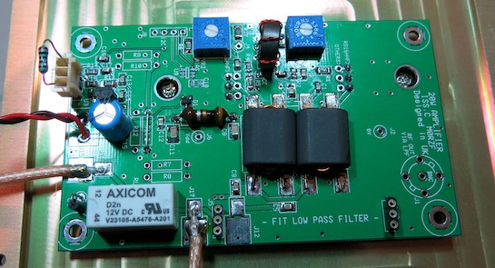
Build Data Release (Iss.C)
NOTE THAT THE BOM HAS BEEN UPDATED TO CORRECT ERRORS AND ONLY LIST PARTS THAT FARNELL/MOUSER HAVE IN STOCK.
Gerber-X files (issue C) are found here. Have a look at them with a free Gerber viewer like PentaLogix SmartDFM. I included top and bottom silkscreen, but to save costs the bottom silkscreen is not essential. Board size is 100 x 60mm. Recommended PCB type is 1.6mm thick FR4, plated through holes, hot air solder level (HASL) finish, 1oz copper. Top and bottom solder masks are required. Any PCB manufacturer who has a clue will accept those files.
The circuit diagram is here, the bill of materials (BOM) is here
NOTE: THE FOOTPRINT OF U2 (78L05) IS REVERSED ON ISS.C BOARDS, and CORRECT ON ISS.C1 BOARDS.
Development & Performance Notes - Mitsubishi FETs
At the outset I spent a while surveying available power transistors, before settling on the RD16HHF1 from Mitsubishi semiconductors. These are used by Icom, Yaesu, Kenwood, Elecraft…
The concept was based on the transformer layout by G6ALU which is functionally equal to other transformer layouts, and uses easily available BNxx-202 twin hole balun cores. I made a first attempt with the issue A board, superseded by the issue B which was sold as a kit. It had many features to interface with Softrock RxTx V6.3 and the Ensemble boards with a few component values different.
The power output was near 20W on the lower bands, dropping to 15W on 28MHz. On my PCB the positions for RD16HHF1 connections are indicated on the silkscreen layer if using a commercial standard PCB. The drain and source pins are reversed between the Mitsubishi FETs and switching types.
When using Mitsubishi FETs, performance is equal to other amplifiers, such as PennyWhistle from HPSDR. The original page for the Pic-A-Star amplifier is still available here. The Mitsubishi FETs are very robust devices. The RD15HVF1 from Mitsubishi is also suitable, and gives slightly better gain at 50MHz.
Development & Performance Notes - STP16NF06L FETs
Switching FETs are much cheaper, but how is their performance compared to the “RF” parts?
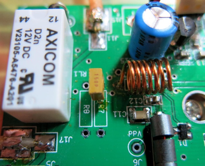
A major physical problem with switching FETs is the tab is drain. So tab is “hot” in voltage and RF terms, but has to be heat-sinked. I recommend a relatively thick heat transfer washer without heat transfer compound.
Before fitting the bias network resistors, check the VGS threshold of your devices. Resistors at top and bottom of the trimpots VR1, VR2 are there to make adjustment easier. So calculate the centre point of VR1, VR2 to be at the point where the device just switches on. Unfortunately switching FETs are designed with a very sharp DC switch-on point, as required in power supplies. This can make the bias unstable. I found the STP16NF06L to be very sensitive to adjust. Despite temperature compensation they will run-away and overheat. Always watch the current drawn by the circuit with a multimeter when adjusting, and observe the variation over several minutes.
An early prototype board undergoing bias adjustment and input network analysis is pictured next:
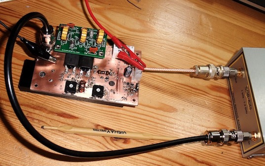
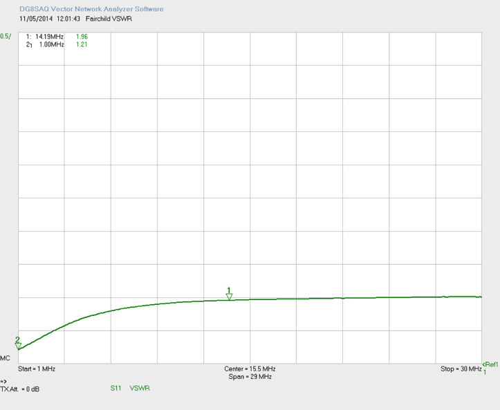
With the TE Axicom relay, quiescent current is 80mA at 13.6V. It is safe to put 200mA quiescent through each MOSFET when heat-sinked. The input SWR and of course the gain is affected by the bias current. Before running power tests, I looked at the response of the Kits & Parts 20m band low pass filter in-situ as in the picture. The first plot shows SWR and S21 (thru) response with the 20m filter plugged in.
The second plot is the input with resistors added to bring up the impedance closer to 50 ohms. It is possible to experiment with the input PI network and achieve better matching, though the input SWR is reasonable and will not be a problem for most driving stages. Certainly the Softrock output stage can drive this without problems. It is worth noting the high SWR on the right of the plot is caused by the low pass filter response, as expected.
The big question is how good is linearity of these FETs in two tone intermodulation? Running into a dummy load with PSK-125 and listening to the signal on a receiver, while varying the power gives a rough idea. The signal sounds the same from power outputs of a few watts up to 25W at 14.070MHz. There is also no detectable splatter with the receiver.
My test equipment does not run to a spectrum analyser. I only have the SDR-Kits VNWA network analyser, which is brilliant at its primary function, but the spectrum analyser has a minimum resolution of 250Hz. I also have no proper signal generator, let alone the two required for an intermodulation test. The best I can do is generate a PSK-125 signal and sniff the output on the VNWA used in spectrum analyser mode.
Overall gain with STP16NF06L is actually higher than RD16HHF1 on the lower bands. If you only want to operate <10MHz they would be better. But see the compensation notes further down this page.
LINK TO TOP OF PAGE
In a PSK-125 intermodulation test, this is the result from the RD16HHF1 amplifier driven to 16W (post filter) on 21.070MHz. Two tones with no characters transmitted during analyser sweep.
Next the result of the STP16NF06 at same power level. The “shoulders” relative to the main signal are lower than the RD16HHF1 result. The “shoulder” is about -22dB and -25dB respectively, representing intermodulation products from the amplifier. The input power at 250mW is well within the Softrock Ensemble PA linear region.
Driving either type to an output of 25W makes the “shoulders” rise up towards the main signals, to within -10dB. This expected result shows the test is a valid one. Surprisingly the cheaper MOSFET has a better intermodulation performance than the expensive “RF” part. The Mitsubishi RD16 die is probably a standard FET die wire bonded differently to get the tab grounded. There is no magic in its construction.
The ST FETs drop off in gain more than the Mitsubishi's as frequency is increased. At low frequencies they will drive to maximum output (>25W) with <0.2W. But at 10m, you will need 0.8W to get 20W out. It is possible to put a compensation network in which will flatten out the gain considerably. With a bit of simulation and testing, the values are:
- A 150pF leaded capacitor at the R7 position. There is a grounded via provided in the middle of the R7 position to fit one leg of the capacitor into.
- A 180nH air spaced inductor at the R1 position. 180nH can be made from 7-8 turns of 22SWG wire wound on a 6mm former.
A picture of the frequency compensation circuit follows.
It is best to start out with 8 turns and adjust the power output on 29MHz. If you find spacing the turns right out increases power, then desolder the coil and remove a turn. Gate capacitance varies widely on these FETs, it is best to adjust your own board individually. Also check the gain on 21MHz is peaked up. With the compensation network, I find the maximum power output to be 25W on 29MHz, with 1.0W input. At 3.5MHz it gives 30W for 0.5W input.
In conclusion, I find the STP16NF06 to be a capable and cheap amplifier device for HF transmitting.
Development & Performance Notes - Fairchild FQP13N06L FETs
An extensive survey of TO220 FETs shows the lowest gate and output capacitance is the Fairchild Semi FQP13N06L. They are cheap, so I tested a pair. With a dummy load, using the Elecraft KX3 as a signal source in FM mode at 0.3W. Quiescent current 700mA combined. Power out was:
7MHz 25W
14MHz 18W
21MHz 14W
29MHz 10W
So the gain drops a lot with frequency which is expected. The gain can be compensated in the same way as for the ST MOSFET. After a lot of tweaking about, I will make the statement that there is nothing to choose between the ST or Fairchild FETS. Bearing in mind the output side is dummy load, the input SWR looks like:
The FQP13N10L is on paper the lowest gate charge TO220 device available. They are often found in the PA stages of 27MHz CBs.
Builder’s Notes
Some of the previous notes are still valid for winding the transformers and setting up. The original builder’s notes file (PDF) is available here. The STP16NF06 or switching FET version only differs in the DC bias (gate) voltage needs to be set lower than the RD16HHF1 version.
The Softrock Ensemble should be arranged to switch the amplifier to transmit by connecting the /PTT line (U4 pin 4) to the J9 pin 1 of the amplifier. So pulling down the base of U3 on the amplifier when the Tx is keyed. Coax input at J11 can be connected straight from the Ensemble RF output. Details of how to terminate coax tails is in builders notes.
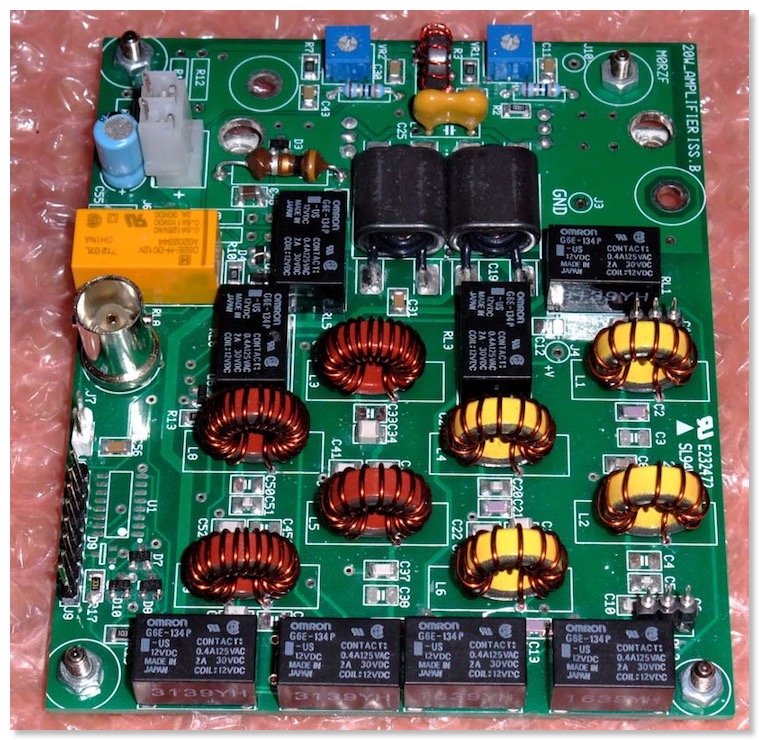
Previous 20Watt Amplifier Issue B (2009)
My previous project was an amplifier with integrated filters, circuit diagram here. Design of HF amplifiers using Mitsubishi RD16HHF1 MOSFETs is old news now. The ones I built in early 2009 are still working reliably. This was the last “issue.B” unit, all of which are now sold !